
Tag Archives: NOR
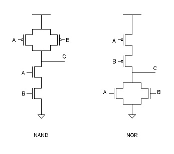
Why NAND Based Design is better than NOR Based Design
Standardi) PMOS in NAND is in parallel while that in NOR is in series
ii) Parallel PMOS makes a stronger pull up network than serial PMOS
iii) Since hole mobility is lesser than electron mobility, NAND-based design is faster than that of NOR-based design (because of parallel PMOS)
iv) t_phl and t_plh (high to low, low to high times) are more symmetric in NAND than in NOR. t_plh of NOR is slower because of the series PMOS.
Implementing Logic Gates with Mux
ImageIt is tough to remember all the Mux to Logic Gate conversion implicitly. So its important to know the method to do the conversion. Here are some steps that will help you with the process,
i) Start with the truth table of the logic gate to be converted
ii) Fix one of the input variables as the Select signal (S) and then decide on what the input signals to the Mux should be so that the Mux satisfies all the cases in the truth table
Example: For AND, Output = 0 for B=0, and Output = A for B = 1.
For XNOR, Output = A’ for B=0, and Output = A for B=1.

Logic Gate Function Tables
StandardHere are some of the basic Logic Gates’ function tables.

|
AND GATE |
||
|
A |
B |
A.B |
|
0 |
0 |
0 |
|
0 |
1 |
0 |
|
1 |
0 |
0 |
|
1 |
1 |
1 |
|
OR GATE |
||
|
A |
B |
A + B |
|
0 |
0 |
0 |
|
0 |
1 |
1 |
|
1 |
0 |
1 |
|
1 |
1 |
1 |
|
NOR GATE |
||
|
A |
B |
(A + B)’ |
|
0 |
0 |
1 |
|
0 |
1 |
0 |
|
1 |
0 |
0 |
|
1 |
1 |
0 |
|
NAND GATE |
||
|
A |
B |
(A . B)’ |
|
0 |
0 |
1 |
|
0 |
1 |
1 |
|
1 |
0 |
1 |
|
1 |
1 |
0 |
|
XOR GATE |
||
|
A |
B |
AB’ + A’B |
|
0 |
0 |
0 |
|
0 |
1 |
1 |
|
1 |
0 |
1 |
|
1 |
1 |
0 |
|
XNOR GATE |
||
|
A |
B |
AB + A’B’ |
|
0 |
0 |
1 |
|
0 |
1 |
0 |
|
1 |
0 |
0 |
|
1 |
1 |
1 |
|
NOT GATE |
|
|
A |
A’ |
|
0 |
1 |
|
1 |
0 |
