I have the basic Read and Write operation of a 6T SRAM Cell below with figures.
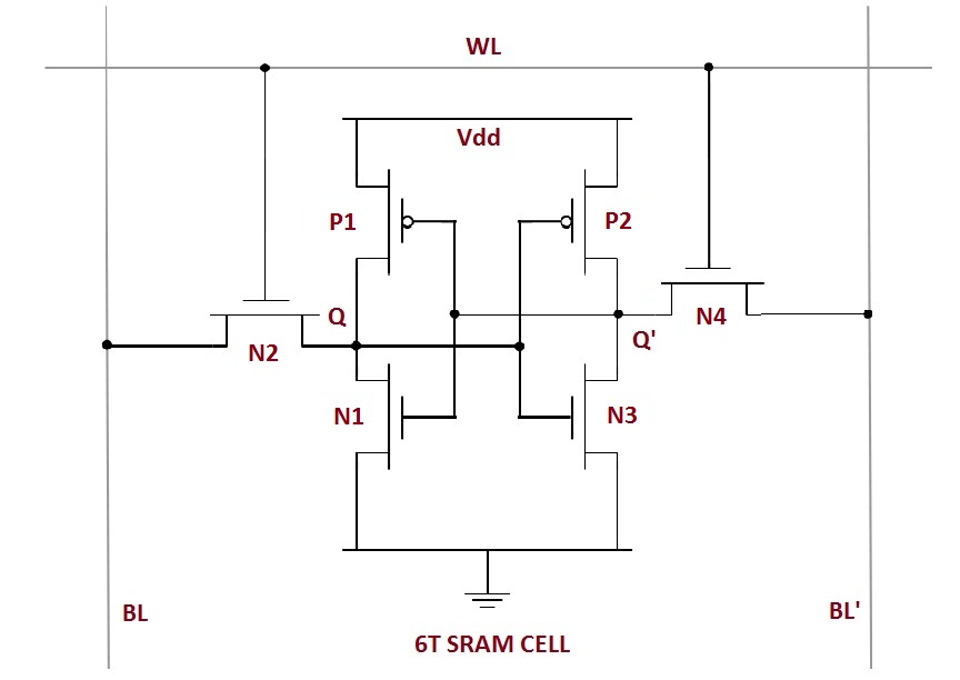

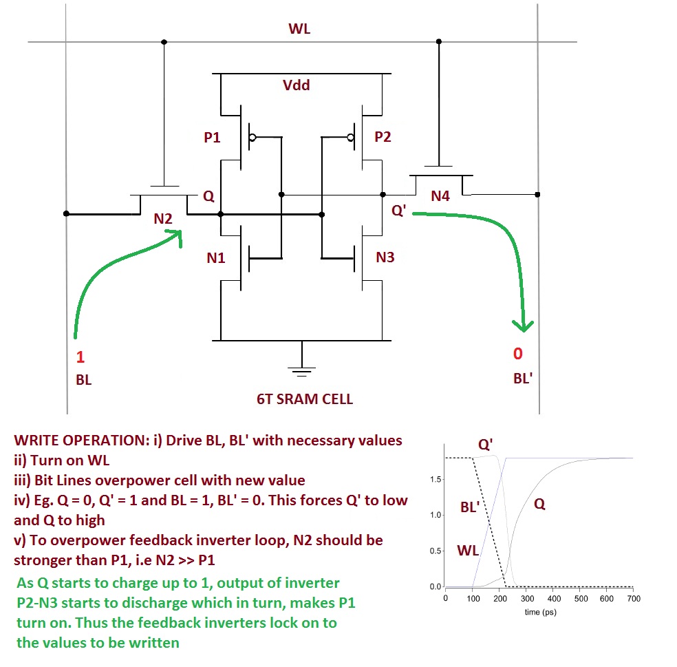
Note: i) N1 >> N2 >> P1
ii) There are other explanations with the transistors named M1, M2 etc. I think the naming convention followed in the material I referred (a lecture I found online) is good because the PMOS and NMOS are distinctly named and that helps remembering the concept better, specially the relative strength of the transistors.
