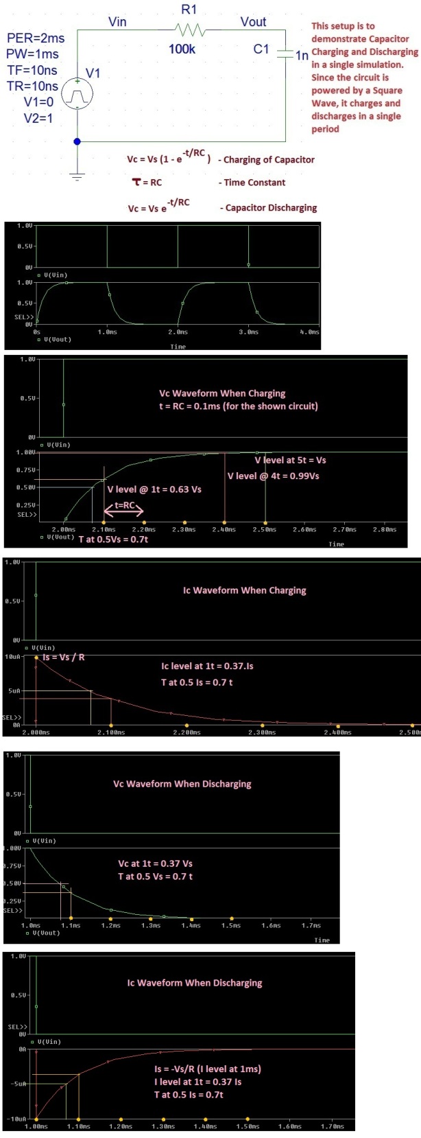
Charging, Discharging a Capacitor
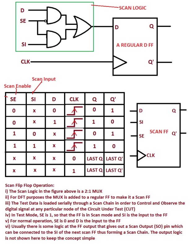
StandardScan Flip Flop Operation
ImageWhy CMOS Logic Should Always Have Vdd Level Input?
StandardThere are several Logic Design Topologies that supply a output voltage less than Vdd level (Pass Transistor Topology for example). If these outputs are fed into a CMOS circuit (to the Gate terminal), there are a few issues that arise with reference to Voltage and Current.
i) VOLTAGE ISSUE: The reduced voltage level at the input might be mistaken by the CMOS circuit to be a logic 0 instead of a logic 1. To fix this issue, the switching threshold of the CMOS circuit should be pushed to a lower level so that it can recognize a lower voltage as logic 1. This entails increasing the Width of PMOS – Wp, so much more than Wn – the Width of NMOS (even beyond the sizing for equal rise and fall times)
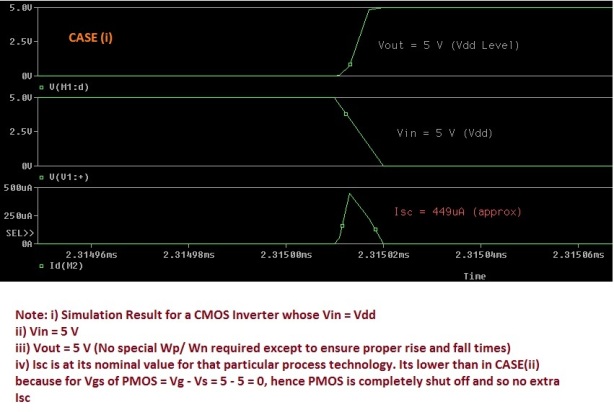
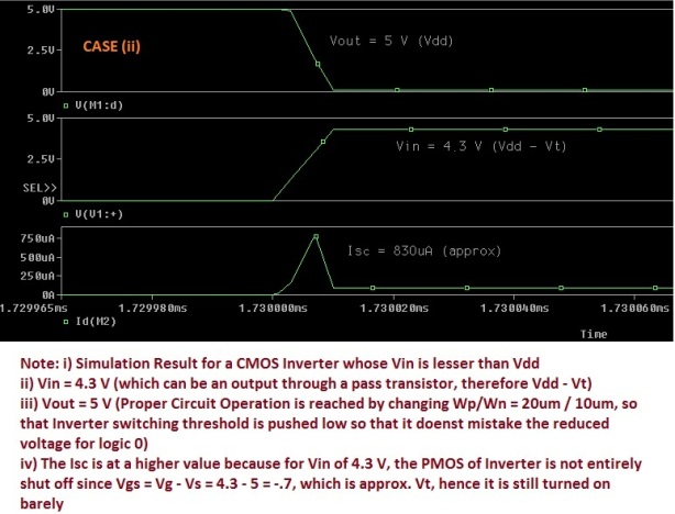
ii) CURRENT ISSUE: The reduced voltage level at its inputs lead to a situation where the PMOS device is not totally shut down. Eg. Let the Vin = 4.3 V and Vdd = 5 V. For PMOS, Vgs = Vg – Vs = 4.3 – 5 = – 0.7 V, which is around Vt for PMOS and hence its not completely shut down and this causes a increase in Isc compared to the case when Vin = Vdd. This is explained in the waveforms shows below.
I simulated an Inverter Circuit using PSpice Demo Version with its rudimentary MOSFET transistors (so I don’t know its Vt). The following are the waveforms that I got after simulating with Case (i) Vin = 5 V and Case (ii) Vin = 4.3 V. In both cases Vdd = 5 V
This simulation makes us understand that in order to use logic styles like Pass Transistor Logic, one need to use additional devices for level restoration so that the output voltage level is same as Vdd .Hope this gives you a deeper insight into CMOS Design.
Leave a Comment if you find this post interesting!
