
Category Archives: VLSI
Basic VLSI Q&As
Why CMOS Logic Should Always Have Vdd Level Input?
StandardThere are several Logic Design Topologies that supply a output voltage less than Vdd level (Pass Transistor Topology for example). If these outputs are fed into a CMOS circuit (to the Gate terminal), there are a few issues that arise with reference to Voltage and Current.
i) VOLTAGE ISSUE: The reduced voltage level at the input might be mistaken by the CMOS circuit to be a logic 0 instead of a logic 1. To fix this issue, the switching threshold of the CMOS circuit should be pushed to a lower level so that it can recognize a lower voltage as logic 1. This entails increasing the Width of PMOS – Wp, so much more than Wn – the Width of NMOS (even beyond the sizing for equal rise and fall times)
ii) CURRENT ISSUE: The reduced voltage level at its inputs lead to a situation where the PMOS device is not totally shut down. Eg. Let the Vin = 4.3 V and Vdd = 5 V. For PMOS, Vgs = Vg – Vs = 4.3 – 5 = – 0.7 V, which is around Vt for PMOS and hence its not completely shut down and this causes a increase in Isc compared to the case when Vin = Vdd. This is explained in the waveforms shows below.
I simulated an Inverter Circuit using PSpice Demo Version with its rudimentary MOSFET transistors (so I don’t know its Vt). The following are the waveforms that I got after simulating with Case (i) Vin = 5 V and Case (ii) Vin = 4.3 V. In both cases Vdd = 5 V


This simulation makes us understand that in order to use logic styles like Pass Transistor Logic, one need to use additional devices for level restoration so that the output voltage level is same as Vdd .Hope this gives you a deeper insight into CMOS Design.
Leave a Comment if you find this post interesting!
Clock Skew
StandardHere is one of several topics I intend to write regarding Timing in VLSI.

Interconnect Delay Reduction Using Buffer Insertion
StandardEver wondered how the propagation delay of an interconnect is reduced by inserting buffers in between? Here is an explanation.

Metastability
Image
ASIC Design Flow
Image
Short Circuit Current in an Inverter
StandardHere is a snippet on Isc of an Inverter.

DRAM – An Intro
StandardSome facts about DRAM
i) Higher density than SRAM (1T vs 6T)
ii) Because of (i), cost per bit of DRAM is lesser than that of SRAM
iii) On the downside, DRAM is slower than SRAM because reading value stored in a capacitor is slower than reading output of feedback inverters of SRAM
iv) Timing and control logic is more complex than SRAM’s
v) Since charge of storage capacitor leaks constantly, DRAM needs refresh cycles in order to maintain data integrity
vi) Since there is no feedback inverter loop for data regeneration, DRAM is a passive memory cell
vii) The data stored in the capacitor can be altered by a lot of factors (leakage, radiation etc) and so the soft bit error rate of DRAM is higher
viii) Because of (iii) to (vii), DRAM can be used as main memory but not as cache memory (SRAM fits the requirements of cache memeory better)

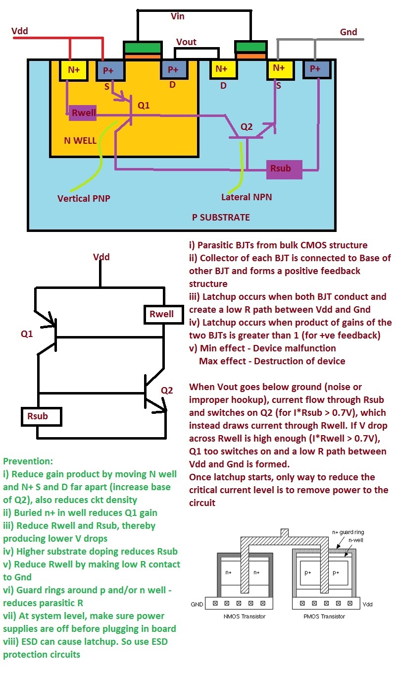
Latchup – Cause, Effect and Prevention
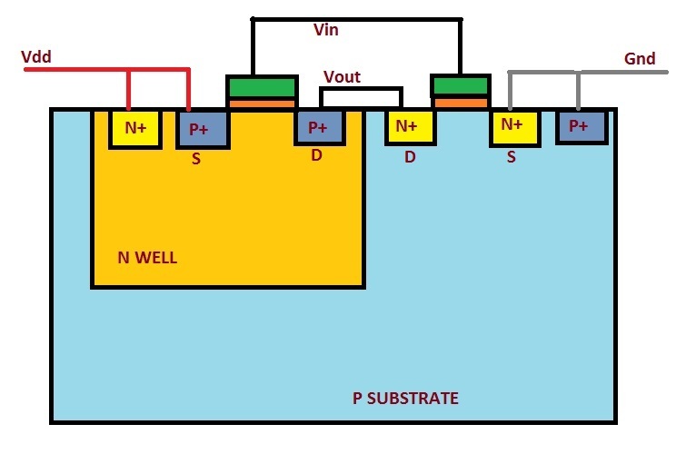
StandardHere is a typical Bulk CMOS device (a simple Inverter)
Now, here is the same figure showing the parasitic BJTs that cause latchup.
Why Transmission Gate NMOS, PMOS is not sized?
StandardIn a Transmission Gate, the PMOS and NMOS are not responsible for the rise time and fall time independently (as in an inverter where PMOS width has a role to play in the inverter rise time). In a TG, both NMOS and PMOS assist each other in conducting input to output because when the control voltages are right, both PMOS and NMOS are conducting else both are off.
