I have come across several Pass Transistor interview questions on the internet, many of them asking to figure our the final output voltage level. In the past, I have gotten confused with the terminals of a pass transistor because in general, transistors are symmetric and the Source and Drain terminals are interchangeable. Here is my explanation for such a problem so that you don’t ever get confused in case such a question is posed.


B is Vg (V at gate)
X is Vs (V at source)
A is Vd (V at drain)
For an NMOS to conduct, Vgs > Vt, so Node X does not charge beyond a point where Vgs < Vt.
Some sample problems. Assume Vt = 0.7 V. Solve and check solutions at the end of the post.
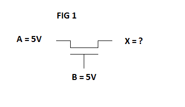
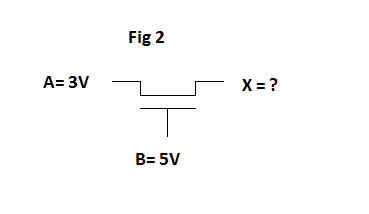

Most questions asked are variation of the basic serially connected or cascaded NMOS structures. If you stick to the basic principle and solve for each node, you will get your final answer right.
Fig 1: Vx = 4.3 V
Fig 2: Vx = 3 V
Fid 3 (un-named): Va = Vb = Vc =Vo =4.3 V
